What are PCB stencils? A Step by Step Guide for Beginners

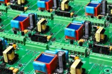
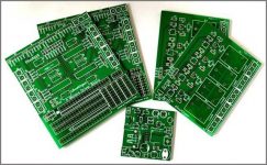
A PCB Stencil is a sheet of stainless steel with laser-cut apertures that we have to use to apply solder paste to a PCB board to insert surface mount components. The PCB stencil has the use to apply solder paste to specific areas on a bare PCB board. So that components can be precisely fitted and aligned. An SMT stencil’s main purpose is to transfer solder paste to a bare circuit board. Every surface mount device on the board has an aperture created by a laser-cut stainless steel foil. The ideal size of the stencil aperture is to fit the PCB’s land area. With a standard stencil thickness of 0.125mm, a pad to the aperture aspect ratio of 90 percent to 100 percent is the best one. PCB stencils are made of metal or polyimide, which is commonly useful for thin sheets. Metal (usually stainless steel) stencils are best for producing a large number of prototypes. Stainless steel stencils enable more precise aperture creation.