A List of Seeed Studio PCB Assembly Sponsorships You Shouldn’t Miss

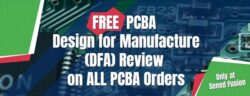
The COVID-19 pandemic significantly affected the offline trade contacts, therefore, lots of companies turn to find PCB assembly partners online in the past year.  Seeed Studio has always been committed to providing companies around the world with faster and higher-quality manufacturing services, their ongoing goal is to assist customers to achieve the best possible time to market and competitive advantage by providing PCB assembly service in a sustainable way at the lowest total cost through competence, delivery accuracy, and product quality. In this piece, we’ve put together a list of sponsorship activities that Seeed Studio offers for their PCB assembly customers. Without further ado, let’s jump right it. Design for Assembly (DFA) Review Now Free for All PCB Assembly Orders with Seeed Fusion Seeed Studio are now including the highly acclaimed Design for Assembly (DFA) review with every PCBA order – 100% free. No prices have been hiked up or additional fees squeezed in anywhere.

Continue reading

What is a double-sided PCB? Best Guide for Beginners in 2021

PCB stands for the printed circuit board. It is a non-conductive material containing printed or etched conductive lines. The board has electronic components on it, and the traces connect them to form a working circuit. It has two common types; single-sided and double-sided PCB. What is meant by double-sided PCB? Double-sided PCBs are similar to single-sided PCBs, except they include two layers of traces, one on top and one on the bottom. Moreover, these circuit boards allow conductive copper and components to be mounted on both sides of the circuit board.

Continue reading

Which is the best prototype PCB Company in 2021?

The prototype PCB board is a product used on a large scale in the electronic market, being applied in different segments from information technology and telecommunications to automotive and aerospace. Which is the most common PCB prototype software? Printed circuit board prototype is one of the most requested services in the electronics industry. It is important to test a prototype board to carry out tests before ordering mass production. We know of several PCB prototype vendors, but we don’t know their features and advantages.

Continue reading

What are the steps in the process of SMT manufacturing?

Surface-mount technology (SMT) refers to the assembly of electronic components using automatic machines that install components on the board’s surface. Moreover, this board is known as a printed circuit board, or PCB. When it comes to electronic assembly, SMT is the most popular method in the industry. JLCPCB is offering very attractive rates for PCB manufacturing and assembly. They are willing to produce 1-4 layer PCB for as low as $2 and additionally, you can get free PCB assembly once a month. This is a great opportunity to check

Continue reading

PCB Assembly Services: Step by Step Guide for Best PCB Assembly

A PCBA (Printed Circuit Board Assembly) is a board that has been soldered and mounted on the PCB and can now perform the electronic function for which it was created. Printed circuit board assembly is one of the most critical processes in PCB production. Moreover, it includes all of the components needed to construct the PCB. SMT and THT are the two ways of constructing a printed circuit board assembly.

Continue reading

What are PCB stencils? A Step by Step Guide for Beginners

A PCB Stencil is a sheet of stainless steel with laser-cut apertures that we have to use to apply solder paste to a PCB board to insert surface mount components. The PCB stencil has the use to apply solder paste to specific areas on a bare PCB board. So that components can be precisely fitted and aligned. An SMT stencil’s main purpose is to transfer solder paste to a bare circuit board. Every surface mount device on the board has an aperture created by a laser-cut stainless steel foil. The ideal size of the stencil aperture is to fit the PCB’s land area. With a standard stencil thickness of 0.125mm, a pad to the aperture aspect ratio of 90 percent to 100 percent is the best one. PCB stencils are made of metal or polyimide, which is commonly useful for thin sheets. Metal (usually stainless steel) stencils are best for producing a large number of prototypes. Stainless steel stencils enable more precise aperture creation.

Continue reading