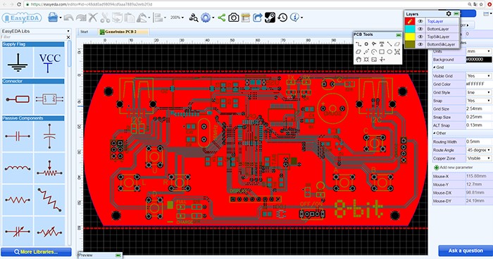
Your electronic circuits come to life in physical form on printed circuit board design. The PCB design process uses layout software to describe electrical connectivity on a printed circuit board by combining component placement and routing.

What are the environmental factors in PCB design?
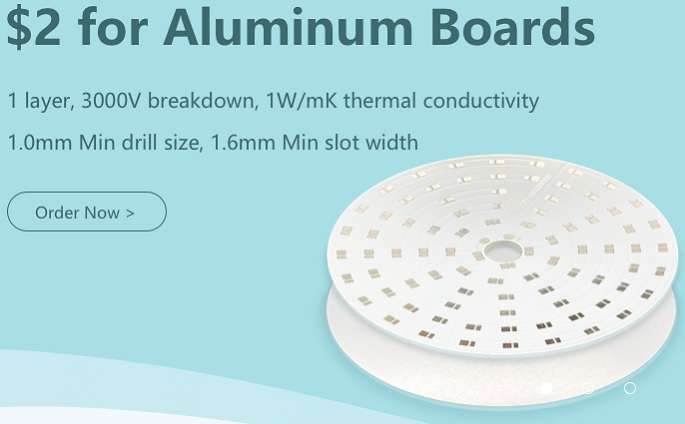
Many variables need to keep in mind when designing PCBs for outdoor use with an enclosure to safeguard the PCB. Temperature, dust particles, vibrations, electrical interferences, and various other environmental conditions such as rain, snow, hail, and vermin are just a few examples. For better heat dissipation, try using aluminum PCBs. JLCPCB offering them from $2
What are the ways to improve layout efficiency in PCB design?
According to JLCPCB, the efficiency of a PCB depends on its design. The way it is designed and implemented determines its future and adds to the long life of its employed device. The efficiency of circuit board design will considerably improve by making tiny adjustments to the design during the layout stage. Here are a few strategies to make your layout more efficient.
1. Take a DIY approach to create schematics
When you make a schematic by hand, you can better understand the placement of the components and how they should be constructed and positioned. There are several pre-programmed tools for creating well-thought-out schematics. You can utilize automatic tools to draw up the schematic once you’ve established design standards.
2. Properly space the components
Though you may be tempted to cram components as close together as possible and marvel at the intricate structure you’ve produced, it’s not really functional. Wiring the components that are too close together will undoubtedly be difficult. As a result, spacing components appropriately apart makes wiring and soldering easier.
3. Do not place traces at the right angle.
It will be difficult for the designer to keep the traces evenly wide if they have a 90° angle. A better angle is 45 degrees, which allows for optimal breadth without cluttering the PCB.
4. Ensure the same orientation while placing components.
Firstly, you should be aware that all components come with pins labeled with numbers logically. Pin #1 is for the upper-left corner, and you must now place components according to a predetermined orientation. Furthermore, this consistent method of component placement makes soldering and subsequent inspection easier to manage without making any mistakes.
Use different wiring directions between two consecutive layers.
It’s critical to remember that the wiring directions in successive layers should be varied while designing the PCB layout. Moreover, if horizontal wiring is utilized on one layer, the subsequent layers should be oriented vertically. In the case of a multilayer PCB, this pattern will be extended to all layers.
Who is a PCB designer?
A PCB designer creates 3D models of circuit boards. He also interacts with engineers to build 3D models of circuit boards. Moreover, he develops PCB design guidelines and draughts blueprints for manufacturers using computer software tools.
What do you know about the first step in PCB design?
Ideation, definition, and validation – all before commencing a design or prototype – are the three most critical first steps in the PCB design process.
What are the PCB design techniques?
To adjust the resistance of a PCB trace, most PCB designers employ length, thickness, and width. The resistance of the metal used to produce the trace is a physical feature of the metal. Because PCB designers can’t actually adjust copper’s physical qualities, that’s why they should concentrate on trace size, which they can regulate.
Is PCB design hard?

The majority of the work is straightforward. It only requires a great deal of attention to detail and adherence to well-established technical guidelines. However, developing that amount of knowledge takes time. Moreover, anything other than a basic 1- or 2-layer board can appear overwhelming to someone just getting started with the PCB layout.
Is PCB design a good career?
PCB design is already a rewarding professional path, and we expect it to improve as PCB technologies become more advanced. When it comes to producing a product and its inner workings, a PCB designer’s role is critical.
How can I be a good PCB designer?
PCB design is already a rewarding professional path. We expect it to improve as PCB technologies become more advanced. When it comes to producing a product and its inner workings, a PCB designer’s role is critical.
A printed circuit board designer’s primary responsibility is to design and test PCBs. A PCB designer works in an office or cubicle, either at an engineering business or a manufacturing site, in front of a computer. The designer’s duty is to use specialist software to construct the board’s functionality.
What is a PCB diagram?
A PCB schematic is a two-dimensional circuit design that depicts the functionality and connectivity of various components. PCB design is the next step after blueprints. The layout, or physical representation, of the PCB schematic, including the copper track and hole pattern, is the design.
How can I learn PCB design online?
Find a CAD package for this purpose; there are several low-cost or free solutions for PCB design on the market. Keep the following considerations in mind while selecting a bundle.
- Examine other people’s designs to see what they’ve come up with.
- Practicing, Practicing, Practicing
- Keep your expectations low.
- Schematics are crucial.
How long does it take to learn PCB design online?
The program consists of two 8-week sessions, the first of which covers PCB design. The PCB at JLCPCB will then be assembled and tested in a separate session. Members are located all around the world, and static and live videos provide teaching.
Although an associate’s or bachelor’s degree may be required for printed circuit board designers, certain employees may not require formal education. Individuals in these professions, regardless of their educational background, need to get skills regarding designing software.
What are the most common problems during the design of a PCB?
There are countless issues with PCB design and some of them are here.
- Starved thermals
- Acid traps
- Silvers
- Insufficient annular ring
- Via in Pads
- Copper is too close to the edge of the board.
- Missing solder mask between pads
- Tombs toning