Multilayer PCB introduced, in which connections or wirings are separated across multiple PCB boards (called layers), laminated, and glued together to keep them isolated from one another. Consequently, any PCB having three or more layers is referred to as a multilayer PCB.
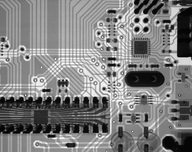
In the last few decades, electronics have advanced at a fast pace. Our cell phone is now a complete computer, which is not conceivable without multilayer PCBs. Moreover, the multilayer PCB is used in advanced electrical devices. It is because it allows for the integration of a high number of components on a single board.
The PCB can be categorized as under:
- Single Layer PCB
- Double Layer PCB
- Multilayer PCB
- Rigid PCB
- Flexible PCB
- Aluminum back PCB
- Rigid-Flex PCB
The need for smaller, more useful electronic devices is increasing all the time. So the multilayer PCBs are the superior alternative for these devices as the size can be minimized by increasing the number of layers..

You can get multilayer PCB or aluminum PCB at JLCPCB for as low as $2.
What are the ways to connect layers on a multilayer PCB?
Layers in the multilayer PCB normally connect in three different styles. A via is a copper-layered hole used to connect different layers of a multilayer PCB in PCB terminology. Vias have three distinct styles, which are here below.
- Through-hole Via. This route runs from top to bottom, connecting all layers of a multilayer PCB.
- Blind Via. This route connects one or more interior layers of a multilayer PCB to any outside layer (top or bottom).
- Buried Via. This route connects to any number of inner levels but never to any exterior layers (top or bottom).
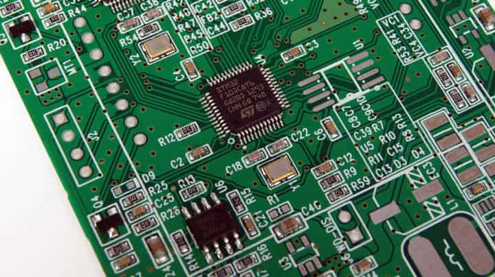
Building a multilayer PCB
Multilayer PCBs are made by connecting all of the layers and materials. High temperatures and pressures are necessary to remove any air present between them. Next, to adhere the components and layers together, resin and adhesive materials are integral. Finally, the PCB is then cooled to create a firm and durable board.
What is the layer stack in a multilayer PCB?
These layers are as below.
- Firstly, the top Layer ( Electronic Components)
- Secondly, the inner Layer (Routing)
- Thirdly, the inner Layer (Routing)
- Fourthly, the inner Layer (Routing)
- Lastly, the bottom Layer (Electronic Components)
What are the major advantages of multilayer PCBs?
Multilayer PCBs offer various design advantages from a technological point of view. Multilayer PCBs have several advantages. Some of them are here:
1. Smaller Size
One of the most well-known and acclaimed advantages of multilayer PCBs is their small size. Multilayer PCBs are intrinsically smaller than other PCBs with equivalent functionality due to their layered construction. This is a significant benefit for modern electronics, as the current trend is toward smaller sizes.
2. Lightweight Construction
The many connectors are necessary to interlink individual single and double-layer PCBs. These are resulting in loss of weight. Again, this is advantageous for current gadgets, which are more geared toward mobility.
3. High-Quality
Multilayer PCBs have a higher quality than single and double-layer PCBs. This is mainly due to the amount of labour and preparation that must go into their fabrication. As a result, they are also more dependable.
4. Increased Durability
By their very nature, multilayer PCBs are long-lasting. These multilayer PCBs must be able to bear not just their own weight, but also the heat and pressure necessary to bind them together. In addition to these issues, the multilayer PCB uses many layers of insulation between the circuit layers, with protective materials tying everything together.
5. Enhanced Flexibility
Though flexible manufacturing techniques are not useful in all multilayer PCB assembly, some do, resulting in a flexible multilayer PCB. This can be a very useful feature in applications where there is a lot of bending and flexing on a semi-regular basis.
6. More Powerful
A multilayer PCB is a highly high-density assembly with numerous layers into a single PCB. Because of the close quarters, boards are more connective, and their inherent electrical qualities enable them to attain higher capacity and speed despite their smaller size.
7. Single Connection Point
Multilayer PCB functions as a single unit rather than in conjunction with other PCB components. Consequently, instead of the various connection points necessary for using multiple single-layer PCBs, they have one. This is especially useful for small electronics and gadgets.
JLCPCB currently is offering a special deal: $2 for 1-4 layer PCBs. Check online quote for more options.

What are the drawbacks of a multilayer PCB?
There are many benefits to the multilayer PCB. On the other hand, it also has some drawbacks. These need consideration before making a final decision to use a multilayer PCB. The Multilayer PCB has some drawbacks, of which some are here for you.
1. High Production Costs
The first is the high cost of manufacturing. The biggest downside of the Multilayer PCB is its high manufacturing cost. Online PCB firms in the world offer low rates. However, the multilayer PCB manufacturing process is fairly good, but it is somewhat costly.
2. Increased Manufacturing Time
A multilayer PCB takes longer to manufacture than a single or double-layer PCB. This is so because it involves extra steps such as printing, laminating, and connecting. Moreover, it depends on the intricacy and quantity of your products, but a simple order usually takes a week.
3. Difficult to Repair
Multilayer PCB is more difficult to debug or repair than a single layer PCB. Since they are pre-assembled and use SMD components. Moreover, companies usually create a prototype to eliminate any flaws or defects before moving on to professional design.
4. Professional Designers Required
Designing a multilayer PCB is difficult because if the model contains a design fault, the manufacturing process must be redone. Consequently, a group of expert designers makes PCB design. Depending on the intricacy of the electronic design, numerous teams may be involved.
Where to order multilayer PCB in China?
Stand out in the electronics sector as JLCPCB that produces quality multilayer PCB and emanates reliability, always looking for products in line with the world trend of cost reduction, protecting the environment and the planet.