A few things to keep in mind can help you create PCB designs that can be manufactured.
- Copper regions – on inner layers, all copper must maintain a minimum 10 m range—moreover, preferably 20 mils, from the board’s outer edge. Check out JLCPCB manufacturing capabilities to be sure.
- By allowing passage through the inner layers
- Ensure there’s enough space around any holes or through barrels with no connection to an inner layer. This clearance should be at least 15 mils, but 20mil is preferable.
- Moreover, for thermal relief pads, the tie must be a minimum of 8mil thick.
- Larger geometries result in higher yields, which are reflectable in the price of your board.
- We can supply thickness specs for some typical materials to help with multilayer board design.
Check to see if the parameters you’re requesting are indeed in need. While departures from traditional “tried and true” formulas are common, each small alteration entails a larger risk, usually reflected in higher pricing, longer delivery periods, and the occasional failure that necessitates a re-design. Moreover, a strategy of an electrical test is useful for multilayer PCB.
Today’s software has aided designers in regularly producing more manufacturable PCBs, and you should expect even better outcomes if you incorporate certain principles into your designs. Once your design is finished, you can order PCB manufacturing and assembly here at JLCPCB for a meager price starting at $2. Also, currently, they are offering $2 for 1-4 Layer PCBs, free SMT assembly monthly
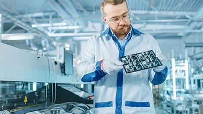
What is the manufacturing process of a PCB?
Like any other process, the PCB Manufacturing process has certain steps to follow. Without following these steps, manufacturing is not possible. These steps are here with concise detail.
1. PCB Designing and Printing:
First of all, you have to design the circuit board before starting the PCB manufacture process. Computer applications such as PROTEL, PADS, and ORCAD, online EasyEDA are useful to finish the design process. It is helpful to create a film that portrays the circuit board’s workings and layers. There are two ink colors to use inside the layers of the board. These are;
Clear Ink:
It is much helpful to show the non-conductive areas of the design.
Black Ink:
Black ink is very fruitful to represent the conductive copper traces as well as circuits. The outside layers will have painted in the same colors as the inner levels. But the meanings will be inverted.
2. Creating Substrate
The substrate, the shielding substance that preserves the parts on the structure together, is formed by securing the materials in an oven. The design from the printed films is etched away after copper is pre-bonded to both sides of the layer.
3. Printing of Inner Layer
After that, a layer of photo-sensitive film as a photoresist needs to apply to the panel. This ensures that the photo films and the photoresist are identical. To help with alignment, hole pins had bored into the PCB. Meanwhile, the plotter’s black ink, which blocks light from reaching the sections that are not supposed to harden, will need to be removed later.
4. Removal of Unnecessary Copper
It’s time to get rid of any remaining copper on the board. In this step, a more powerful chemical preparation will eat away at the undesired copper. Furthermore, another solvent will complete this procedure, and the board now has the copper substrate required for the PCB.
5. Optical Inspection
The alignment of the freshly cleaned layers must be checked. The layers are positioned in an ophthalmic punch apparatus, which helps to drill a pin over the holes to retain the inner and outer layers aligned. Following the optical punch, the panels are automatically inspected for faults using the equipment.
6. Lamination and Pressing of Layers
The process of lamination needs heat and pressure for bonding epoxy amongst the layers. Moreover, lamination is fruitful in holding the layers together. Pressing of layers makes the layers fix to their proper place and give it shape.
7. Process of Drill
An x-ray finder identifies the drill target locations to locate their location. The stack then secures with proper registration holes before a succession of more particular holes drilled. The drilling file from the original design is then fruitful by a computer-driven machine to locate the right areas to hole. It drills over one hundred bore intact spots of a circuit board using air-driven spindles.
8. Process of Plating and Deposition
The individual layers fuse using a chemical solution. Moreover, the walls of the holes are totally undercover, or plates, by the copper bath. At the same time, a new coating of copper applies to the entire panel, and the new holes need to cover. Finally, computers will control the entire dipping, removal, and procession procedure.
9. Imaging of Outer Layer
The only difference between this step and step number 3 is that we use PCB design to picture the panel’s outer layers. A generator fires high-intensity UV light at them, hardening the photoresist. After that, the panel will go through a machine that will remove the unhardened resist that the black ink has protected.
10. Etching and Plating Step
Here in this step, the panel gets a coat with a tinny copper coating. Furthermore, the panel is tin-plated to allow all of the copper presents on the board. Furthermore, chemical treatments remove the undesirable exposed copper, whereas tin protects the valuable copper during this stage. The connections and conducting regions have now been established.
11. Application of Solder Mask
Before applying the solder mask through SMT Stancil, make sure all of the panels are clean. Moreover, epoxy is fruitful with solder mask film. It is the cause of creating green color on a PCB. UV light will be useful to remove any undesired solder masks. In comparison, the rest will be baked onto the board.
12. Silkscreening and Surface Finishing
After silk screening, the PCB goes through a final coating and curing procedure. Furthermore, the PCB needs to plate in either a solderable or non-solderable finish. We chemically treat the PCBs with gold or silver to increase their solderability. During this stage, some PCBs require hot air-leveled pads. As a result of the hot air leveling, the pads will be uniform.
13. Testing
In this step, an electrical test on the PCB. The automated procedure will confirm the PCB’s functioning and compliance with the original blueprint design. After that, the circuit boards were cut out of the original panel.
How to order PCB manufacturing online?
Buying a printed circuit board from a qualified factory is the ideal choice for electronics manufacturers who ship their products to industry and commerce. JLCPCB has a 24/7 hour online service, over 99% customer satisfaction rate, has the highest repurchase rate. Check the Quote form for more details.