PCB stands for the printed circuit board. It is a non-conductive material containing printed or etched conductive lines. The board has electronic components on it, and the traces connect them to form a working circuit. It has two common types; single-sided and double-sided PCB.
What is meant by double-sided PCB?
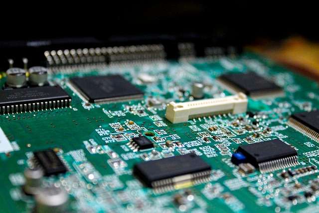
Double-sided PCBs are similar to single-sided PCBs, except they include two layers of traces, one on top and one on the bottom. Moreover, these circuit boards allow conductive copper and components to be mounted on both sides of the circuit board.
What is the difference between single-sided and double-sided PCB?
A substrate is the only layer of foundation materials on single-sided layer boards. On the other hand, a double-sided PCB has two layers that are more layers than a single-sided board but fewer layers than a multi-layer board. So the difference is only based on layers of PCB.
What are the names of the two sides of a PCB?
A circuit board with copper on both sides is remembered as a double-layer PCB. It is also known as double-layer PCB. It’s one side is referred to as the Top Layer and the other as the Bottom Layer. The component surface is the top layer, whereas the component soldering surface is the bottom layer.
How does double-sided PCB work?
These PCBs contain a single layer of base substrate with conductive layers on both sides. On both sides of the board, a solder mask is put. Circuits on one side of the PCB can connect to circuits on the other side to conductive holes in the board. Both sides of electronic components are soldered.
How to Make Double Sided PCB?

First of all, keep in mind that it’s easy to make a double-sided PCB. The steps to make a double-sided PCB are as follows:
- Firstly, create the PCB’s top and bottom layouts using any PCB design program or CAD tool
- Secondly, print both layouts on high-quality glossy paper separately
- Then, cut a Double-Sided Copper plated fiber glass PCB substrate to the desired size and dimension.
- After that, iron the Top PCB Layout Print on the Top Side of the Board using a Cloth Iron (Max Temperature). This may take 20-30 Seconds
- Then, using a scrubber, remove the iron and the laser ink from the PCB Tracks.
- Drill the holes for the relevant components.
- Clean the opposite side of the board now.
- Print the bottom layout of the PCB by repeating Steps 4–5. Ensure that the layouts on both sides are in appropriate alignment.
- Soak the board for 20-30 minutes in a copper chloride solution (CuCl3 or FeCl3) to remove the copper.
- Use conductive ink or a conductive pen with a fine tip to make the Holes Conductive or Plated Through Hole
- Cover all sides of the board with Green Solder Mask.
- Solder all of the electronic components together.
- Now is the time to act — your double-sided PCBA is ready. Have fun with it.
What are the benefits of Double Sided PCB?
Double-sided printed circuit boards are a little more complicated than single-sided PCBs, but they have a few advantages:
- Firstly, it gives you additional options.
- At second, a higher density of circuits.
- Third, the size of the board has been reduced.
- Then, maximum utilization of available space because we can place components on both sides of the board.
- We may employ it in a wide range of electronic gadgets.
- People can design more complex projects.
- Finally, it is economical.
What are the uses of double-sided PCB?
Double-sided printed circuit boards provide higher circuit density and versatility. This is the reason for using these boards by numerous electrical companies throughout the world in a variety of electronic devices and gadgets:
- Converters and a backup power supply
- Power conversion and control relays
- LED lighting and HVAC
- Industrial controls and instrumentation
- Regulators and power supplies
- Traffic management system
- Machines that sell things
- Test and monitoring equipment, as well as line reactors
- Phone systems and printers
- Dashboards in automobiles
Will we call double-sided PCB when it has traces on both sides but connections on one side?
In this case, the PCB has trances on both sides. But the components have a connection on only one side of the board. Yes, even though components only appear on one side of the board, we still refer to it as a double-sided PCB since trances will appear on both sides.
What is the soldering process in double-sided PCB?
Soldering two-layer boards is a time-consuming operation. However, you can use a pick and place machine to solder your board faster than soldering by hand. Moreover, you can also do using CNC Milling Machine.
Advantage of Double Sided PCB
In terms of flexibility and convenience of usage, double-sided PCB is an excellent choice for most experts. When compared to multilayer complex PCBs, we come to the following results:
- It has a higher circuit density
- It is less expensive
- Reduced board size allows for the development of double-sided PCBs
- Lowering total costs
- You can utilize Proteus Ares to design your PCB
- A double-sided PCB is a good choice because it has both top and bottom layers.
- The bottom layer can be used as a ground copper pour.
- Any of the top 10 PCB Designing Software can help you create your own PCB design.
Application of double-sided PCB
Double-sided PCBs have a moderate level of complexity and are commonly employed in a wide range of applications. They are particularly beneficial when a single layer or multilayer PCB fails to meet the project’s requirements.
Where to buy double-sided PCB board in 2021?
Victory PCB Technology Company is a China PCB supplier specializing in the urgent production of double-sided printed circuit boards. You can place an order by visiting our office or online.
When ordering printed circuit boards used in critical areas of electronics (instrumentation, telecommunications technology, industrial automation, the Internet), the first place should always be the quality of products, since a printed circuit board is the basis of any electronic device and its cost is relatively low.