What is ARM?
A well-known manufacturer of microprocessors, ARM (Advanced RISC Machines) is responsible for the design of numerous high-performance, low-cost, low-power RISC CPUs, as well as associated hardware and software. The ARM architecture, which offers a variety of cores, system extensions, microprocessors, and system-on-chip solutions, with four functional modules available for manufacturers to configure production according to the needs of various users, is the first RISC microprocessor created for the low-budget market. It is essentially the industry standard for 32-bit microcontrollers.

The same software can run in all products since they all share a common software architecture. Since ARM presently controls more than 90% of the handheld device industry, it can significantly speed up application development and testing while simultaneously lowering R&D expenses.
ARM is a 32-bit microcontroller that belongs to a part of an Embedded IC with high-performance internal hardware resources that can be loaded with an operating system to become its primary feature. With an operating system, it can multitask in real time like a PC, which means that it can finish multiple tasks at once without interfering with each other.
ARM Architecture
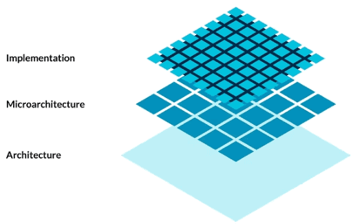
The Arm architectural family is one of the reduced instruction set computing (RISC) architectures used in computer processors. It is the most widely used processor architecture in the world, with more than 250 billion Arm-based chips delivered by our partners over the past three decades in products ranging from sensors, wearables, and smartphones to supercomputers. The Arm CPU design has many benefits, including integrated security, great performance, and energy efficiency, a big ecosystem for global support, and pervasiveness across markets and locales.
What is FPGA?
FPGA, a form of semi-custom circuit in the field of Application Specific Integrated Circuit (ASIC), tackles the dearth of bespoke circuits and overcomes the disadvantage of the initial programmable devices’ limited number of gates. It is not overdone to say that FPGAs are capable of performing the functions of any digital device, from high-performance CPUs to simple 74 circuits, and can be implemented as a piece of paper or a group of building blocks. We can validate the accuracy of the design using software simulation.
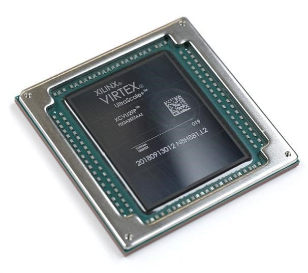
It is also possible to change the design at any time after the PCB is produced using the FPGA’s online editing feature without affecting the hardware circuit. When utilized to develop digital circuits, FPGAs can considerably reduce design time, PCB area, and system reliability. Since on-chip RAM programs are used to set operational states, programming the RAM is required for FPGA operation. Depending on the setup mode, users can employ various programming methods.
FPGA Architecture
Tens of thousands of fundamental configurable logic blocks (CLBs), which are linked together by a network of programmable interconnects known as a fabric, make up a rudimentary FPGA design. Input/output (I/O) blocks form the interface between the FPGA and external devices. Depending on the manufacturer, the CLB may also be referred to as a logic block (LB), a logic element (LE), or a logic cell (LC).
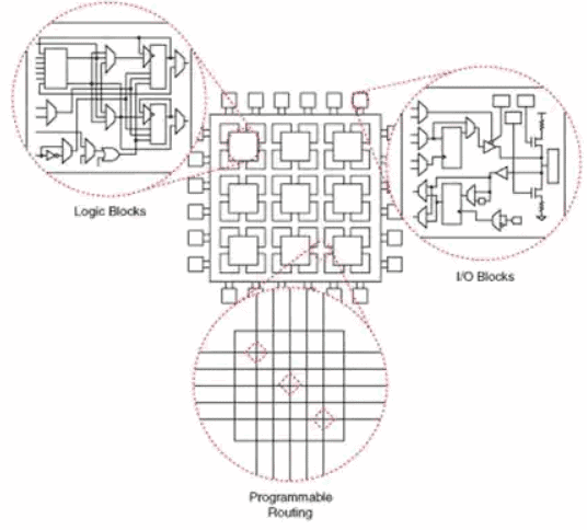
A single CLB is made up of several logic blocks. The lookup table (LUT) of an FPGA is one of its distinctive features. A LUT stores a predetermined list of logic outputs for any combination of inputs; LUTs with four to six input bits are typical. Flip-flops, complete adders, and multiplexers are a few examples of popular logic operations. The more sophisticated CLBs present in current-generation FPGAs may conduct many operations with only one block and can be linked to carry out more complex functions like multipliers, registers, counters, and even operations for digital signal processing (DSP).
How does FPGA work?
When the power is connected, the FPGA chip reads information from the EPROM into the on-chip programming RAM, and once the configuration is finished, the FPGA enters the working state. Because it doesn’t require a special FPGA programmer but rather a general-purpose EPROM or PROM programmer, the FPGA can be used frequently. When the FPGA function needs to be modified, only one EPROM needs to be replaced. This allows the same FPGA to perform many circuit tasks using various programming data. Therefore, there are numerous applications for FPGAs. FPGA chips are among the best solutions for small-volume systems to improve system integration and longevity.
What are Digital signal processors?
DSPs are specialized microprocessors that use digital signals to process a large amount of data. They have a complete set of their own instructions. Its Harvard bus architecture and specialized internal hardware multiplier for handling a lot of digital information quickly are its most important characteristics. A control unit, a processing unit, a variety of registers, and a number of storage units are some of the components of a digital signal processor on a tiny chip. Additionally, its perimeter has the ability to link to various memories and interact with many other devices.
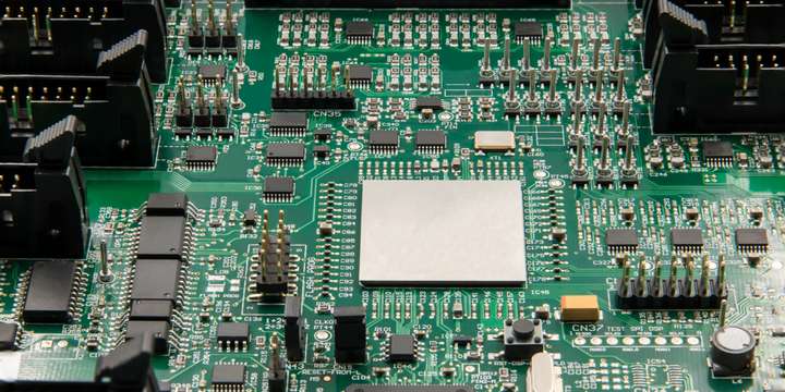
Since the data bus and address bus are divided, allowing program and data to be stored in two different locations, the Harvard design utilized by the DSP allows for complete overlap between fetching and executing instructions. As a result, the microprocessor may carry out the prior instruction while both fetching and decoding the subsequent instruction, greatly enhancing processing speed. The device’s increased adaptability allows for the transmission of data and programs. It works by ingesting analog impulses, converting them to digital signals of 0 or 1, and then adding to, subtracting from, and altering the digital signals. The digital data is finally decoded back into analog data or the actual environmental format by other system components.
DSP Architecture
The super Harvard architecture of DSP is shown in the accompanying diagram. Super Harvard Architecture, abbreviated as SHARC DSP, is the name Analog Devices assigned to its new ADSP-211xx and ADSP-2106x generations of DSPs to describe how they operate inside. To increase throughput, some features were introduced to this architecture. The digital signal processors built using the super Harvard architecture are optimized in a variety of ways, but an instruction cache and an I/O controller are significant enough to be included.
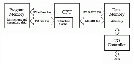
ARM vs. DSP vs. FPGA Features
ARM Features
- loading/storing architecture
- Comprehensive security
- A set of orthogonal instructions
- Only one cycle of execution
- Execution states for 64 and 32 bits that are energy efficient
- Support for hardware virtualization
DSP Features
- In a single instructional cycle, one addition and one multiplication can be finished.
- program and data areas that are separate, giving access to both data and instructions at the same time.
- possesses rapid on-chip RAM that can often be accessed in two independent blocks at once via different data channels.
- hardware support for loops and jumps with little to no overhead.
- fast hardware I/O support and interrupt management.
- Several hardware address generators run concurrently.
- the capacity to carry out several processes simultaneously.
- support for pipelined operations, which enables the concurrent execution of tasks including fetching, decoding, and execution.
FPGA Features
- Configurable logic blocks
- Programmable interconnects
- Programmable routing
- Programmable I/O blocks
- On-chip memory
- Digital Signal Processing (DSP) blocks
- System-level interconnect
- Designing ASICs using FPGAs
ARM vs. DSP vs. FPGA
| ARM | DSP | FPGA | |
| Characteristics | The Arm architecture specifies a set of rules that govern how the hardware responds to a given instruction. The agreement between the hardware and the software outlines their working relationship. | Underpowered and inflexible computer hardware. The quantity of DSPs must be raised in order to enhance the system’s performance capabilities. | It is a working system with scalable computing capabilities because of the adjustable hardware, built-in memory, and integrated CPUs. |
| Programming language | Assembly language is a type of low-level programming language. The assembly language instructions (mnemonics) and the actual binary opcode that the core performs correspond one to one. | C, an assembly language, is used for DSP programming. | HDL, a hybrid digital and analog description language that comprises VHDL, Verilog, and Verilog-AMS, is used by the majority of FPGAs. |
| Cost | RISC CPUs with high performance, low cost, and low power. | Application-specific DSPs are more expensive compared to general DSPs, which are quite inexpensive. A DSP reconfiguration is similarly expensive. | Through customization, several applications can be made to work with FPGAs. They are simple to use since they are adaptable. |
| Applications | Arm processors are extensively used in consumer electronics including smartphones, tablets, wearables, and other mobile devices. They are also used in a wide range of sensors and IoT devices. | Systems that perform complex multi-arithmetic workloads, operate under several conditions, use C programming, and make use of floating point are all ideal for DSP. It is also appropriate for systems that function in a variety of circumstances. | Uses for FPAG include block diagram programming, fixed-point computing, systems with high data rates (a few MHZ), and systems with rapid sampling rates. |
Conclusion of ARM vs. DSP vs. FPGA
The main feature of ARM is that it can be loaded with an operating system, which enables it to perform multiple tasks simultaneously and without crashing. ARM is now divided into two 32-bit and 64-bit versions, each with high-performance internal hardware resources. The benefits of ARM are mostly seen in the control, where it can be utilized to execute interfaces and programs and has rather robust transaction management capabilities. The other won’t have an effect on either. The majority of computing operations including modulation and demodulation, encryption and decryption, etc., are performed using DSP. Advantages include the high data processing capacity and quick operation speed.
FPGAs provide thorough design development and verification because of their flexibility and ability to program, debug, reprogram, and repeat procedures. Small circuit adjustments are the greatest way to demonstrate the advantages of FPGAs, and their ability to be programmed in the field can increase product shelf life and be utilized for system upgrades or debugging.
While FPGA uses hardware to implement data processing, DSP is a general-purpose signal processor that uses software to do so. FPGA is suitable for engineering use with a simple control function algorithm and contains a lot of repeated calculations, whereas DSP is suitable for engineering applications with a complex control function and contains a lot of calculation tasks. FPGA has good real-time and higher cost. FPGA employs hardware whereas DSP uses software to implement algorithms. As a result, the FPGA will process information more quickly. FPGA can conduct parallel computation, but DSP generally requires software to extract instructions for execution, which is still serial execution, and this is a significant reason why it is faster than DSP.
