Many electronic products you use today would not be possible without the innovation of Printed Circuit Boards or PCBs. The Printed Circuit Boards have helped in reducing the size of electronic products and made the product cost-effective.
Below is a summary of what PCBs are, why they are widely used, the types of PCBs to consider, and the manufacturing process of the boards.
What is PCB?
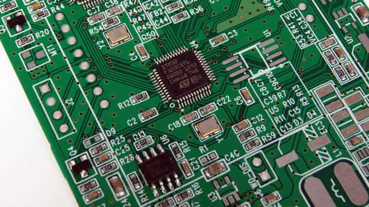
PCB or Printed Circuit Board, are also known as Printed Wiring Board or Printed Wiring Card. It is a vital element in any electronic device.
A Printed Circuit Board is an electronic circuit of a conductive and insulating layer. It offers mechanical support and electronically connects electrical components using conductive tracks, pathways, or signal traces imprinted from copper sheets coated onto a non-conductive substrate.
Since PCB holds the components together, the design mainly depends on the complexity of the circuit or the product. For example, a single layer is used if it is a simple circuit.
But as the complexity intensifies, a double layer board or a multilayer board is used. A complex PCB design helps in reducing the chances of errors and the possibilities of short circuits.
Printed Circuit Boards play a vital role in modern technology. They are the foundation of any electronic product since they are used in almost every gadget.
Being the heart of electronic devices, you will find them in consumer electronics, medical gadgets, industrial applications, automotive applications, etc.
Why are PCBs widely used?
Printed Circuit Boards are the critical components of electronic devices. A lot of people use them for various reasons. Below are some of the reasons why PCBs are widely used.
1. Durability
One of the main reasons PCBs are widely used is that they are durable. Some years back, there was a major complaint in the industry about the boards since they lacked structural strength. But the introduction of these printed circuits has made damage to the boards impossible.
2. Versatile & Adaptive
Another reason why PCBs are widely used is that they can be found in a wide range of applications, including toys, household gadgets, automobiles, space applications, and many others.
3. Cost-effective
When produced on a large scale, the cost of production is very minimal. This has also made the cost of manufacturing appliances go down. This is the main reason why most electronic devices are now affordable.
4. Energy Efficient
Many people prefer PCBs because they are energy efficient. The way they are created, they are highly effective and efficient compared to the traditional circuits.
Type of PCBs
There are many types of PCBs. Each type has its material types, manufacturing specifications, and usages. Below are the main types of PCBs.
1. Single Layer PCB
Single-layer PCBs or single-sided PCBs are some of the most used circuit boards. This is because they are simple to design and manufacture.
A single-layer PCB is made of a single layer, where one side of the PCB is coated with a thin layer. Hence, only one side of the PCB connects different types of electronics.
Some of the single-layer applications include radio, calculators, printers, and other simple devices.
2. Double-Layer PCB
Double-layer PCB or double-sided PCB is another simple printed circuit board. However, it is a bit more complex than a single-sided PCB. It has a thin conducting material applied on both sides of the board.
These boards are usually used in various applications such as industrial controls, AC systems, LED lighting, power supplies, amplifiers, vending machines, and many others.
3. Multilayer PCB
A Multilayer PCB has more than two layers. Hence, it has three or more conductive layers of copper.
The board is secured together using specialized glue and then squeezed in between insulation layers. This is to make sure excess heat does not damage the component of the circuit.
Due to the complexity of their design, Multilayer PCBs are used in complicated devices. It is possible to find a multilayer PCB with more than 12 layers thick.
Some of the applications used by Multilayer PCBs include GPS technology, data storage, file servers, satellite systems, medical equipment, and other devices.
4. Rigid PCB
A rigid PCB is made of solid material, making it hard for the board to twist. One common Rigid PCB is the computer motherboard.
You can find single-layer rigid PCBs, double-layer rigid PCBs, and multilayer rigid PCBs. Since they are simple to design, they are mainly manufactured and used. Moreover, the lifespan of a rigid PCB is very high.
5. Flexible PCB
Flexible PCBs or Flex PCBs are made of materials that can easily bend. Hence, it is a type of PCB that you can flex or twist.

Like rigid PCBs, you can find single-layer flexible PCBs, double-layer flexible PCBs, and multilayer flexible PCBs.
Flexible PCBs come with numerous benefits over rigid PCBs. But the main advantage is the fact that they are flexible. You can fold them over edges and wrap them around corners.
You can find flex PCBs in various applications such as flex solar cells, cellular telephones, LCD fabrication, and electronic devices such as laptops.
6. Flex-Rigid PCB
The other type of PCB is Flex-rigid PCB, a combination of flex PCB and Rigid PCB. The boards contain several layers of flexible PCBs fixed to some rigid PCB layers.
Even though they are not commonly used, they have numerous advantages over rigid PCBs and flexible PCBs.
For instance, flex-rigid PCBs use fewer parts than rigid PCBs and allow a more reorganized design. This helps to reduce the board size and weight.
Some of the applications of flex-rigid PCBs are digital cameras, smartphones, automobiles, and many others.
The manufacturing process of PCB
- Designing the PCB – the first manufacturing process is the design, where there are several design tools you can consider.
- Design review – The next step is to check for potential PCB design errors.
- Printing the design – after checking the errors, the next step is to print the design.
- Etching – this is removing unprotected copper from the board.
- Layer alignment – after etching, the PCB layers go for layer alignment and optical inspection.
- Laminating the PCB layers – now the PCB layers are together, ready to be laminated.
- Drilling– the X-ray machine locates the drill spots, then a CNC drilling machine will be used to drill the holes.
- PCB plating – once the panel has been drilled, it is then plated using a specific chemical. The chemical helps to fuse the layers of PCB.
- Finishing the PCB – the finishing step depends on the type of PCB and the design. In this step, the board needs to be plated with several conductive materials such as immersion silver, hot air solder leveling, and hard gold.
Final Word
PCBs have become vital elements in modern electronic devices. Today, a PCB is used in simple toys to complex medical devices. Hence, printed circuit boards play a significant role in modern technology.
Nevertheless, it is essential to learn about PCBs, the manufacturing process, and the best ones to consider for your application.