PCB design is one of the essential steps in the making correctly functioning electronic device. When drawing a circuit layout, you are making sure that proper components are selected, passives calculated and tested with circuit simulator or test setups.

On the PCB, those components are physically placed, but interconnecting between them relies on design. The more complex circuit gets, the more possible mistakes can occur. Let’s go through several crucial design mistakes and discuss how to avoid them.
Selecting a weak circuit and PCB design tool
There is plenty of PCB design software available. It is vital to choose the one which suits best design requirements. Usually, design tools are used due to company preference, cost, previous experience and recommendations. None of those reasons guarantees that the selected package is optimal.
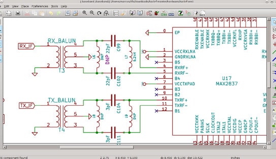
Selecting wrong tools may lead to additional problems, such as delayed times of designing and increased manufacturing cost. The best advice is to do a thorough analysis of available tools. The critical points of comparing EDA software packages are:
- Support
- Level of automation
- Interface
- Supported formats
- Libraries
- Cost
- Mixed simulation
You can think of more criteria. You should apply them to your design needs and then select the one which suits you best. Among most popular tools you can start checking Altium Designer, Autodesk Eagle, KiCad EDA, SolidWorks PCB, OrCAD, ExpressPCB Plus, DipTrace.
Every PCB manufacturer offers free online Gerber Viewer to check if your design files are exported correctly.
Lack of competence in layout
Laying a high-end PCB requires skills that are learned by only doing and learning. Modern electronics are small size and complex. Increased clock speeds and smaller sizes bring a challenge in tracing good PCB. Where there are high signal speeds, the physical characteristics of the circuit board is impacting signal characteristics. Due to the design flaw, the signals may get distorted, delayed and affected by generated noise.
If earlier PCBs were more focused on component placing and routing, today it is more focus on where to place components and where and what shape traces will be physically placed. PCB itself is more electronics component than carrying armature.
General PCB layout recommendations to reduce most of the problems are:
- Fine-tune component placement
- Organize proper power, ground & signal traces
- Keep digital and analogue things separate
- Take care of thermal issues
- Always checking layout against PCB design rules
Improper selection of PCB materials and sizes
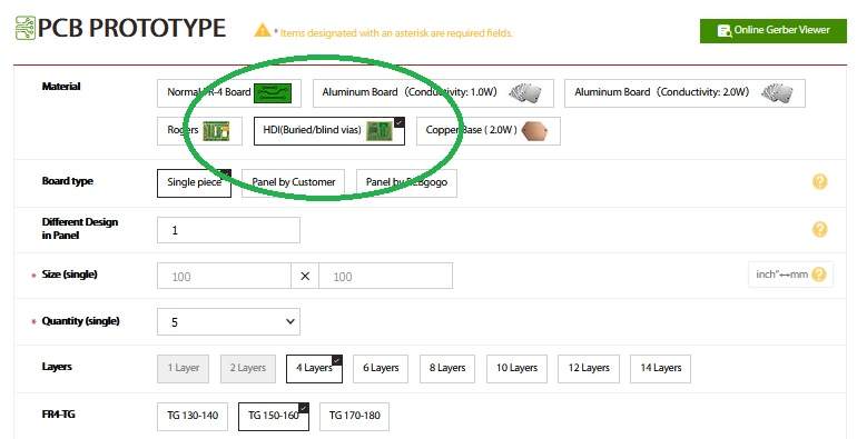
If you look at default PCB settings of any PCB manufacture, you will see that by default copper thickness is 1 ounce per sq. Ft. Depending on signal power and thermal requirements, you may find that this may not be enough. Before tracing PCB, you should be familiar with the power and thermal properties that would allow selecting proper copper thickness or even different base material such as aluminium or copper. Also depending on those parameters, your traces might need to be wider than other signal lines.
Poor communication
Most of the power and thermal related issues you can avoid if you design circuit and PCB. If you work in a team, it is essential to specify the requirements so other members would understand and could easily apply in following steps of operation. Excellent communication between designers and teams will ensure faster operation times and guaranteed delivery times.
Ensure that design is reviewed not only by you but all competent team members. One person cannot be sure to spot all problematic elements. Reviewing during designing may significantly reduce delivery time.
Back-up your work

It may seem insignificant, but periodically backing up your data may save you in case of prominent failures, such as hardware malfunction or data corruption. If you’ve been working on EDA design for weeks, and you accidentally lose your work, you would not want to start from scratch. Make sure to back your data into portable media and also upload to the cloud storage. You can use version control tools for larger projects, or apply your versioning by naming file archives so you could track down last good copy.
Avoid basic PCB mistakes
During PCB design and layout, it is common to make various mistakes that cannot be spotted until you start production. Let’s go through most common.
Incorrect component footprints
Most of Eda packages come with larger or smaller libraries where you can find most of components and footprints. There should be no problem if you select the element from standard libraries, but often there are cases where the designer needs manually to draw component landing pattern. A simple mistake in footprint can leave you scratching your head for some time. Be sure to make the exact matching of pins even at fractions of millimetres. Don’t afraid to print newly created footprints on-page and physically check compatibility.
Decoupling capacitors placed improperly
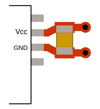
Decoupling capacitors are critical to ensure a clean and sustainable voltage source to individual components. Decoupling capacitors are placed on power rails very close to component power pins. There are many situations when caps are scattered far from critical components and doing more damage than use.
Too narrow for power traces

PCB copper traces are skinny and this is very important to know the current flowing through them. The width would be selected depending on current, copper thickness, where the trace is located (internal or external layer). An outer layer can carry higher currents than internal because it dissipates power better. Usually, a god EDA has a trace width calculator which gives you width depending on the current size, safe temperature rise, and other parameters.
Blind/buried vias not manufacturable
Probably this problem is not very critical as most of the manufacturers are capable of adequately making blind or buried vias. A typical through-hole vias go through all layers of the board. This means even if you only want to connect a trace from layer one to layer two, that all of the other layers will also have this via. A blind via connects an external layer to an internal layer, whereas a buried via connects two inner layers. However, they have strict limitations on which layers they can be used to connect. Be sure to check manufacturer design guidelines where you can see he is capable of making this type of interconnections.
Just know that using blind and buried vias significantly increase PCB manufacturing costs. Use them only if necessary.
Choosing a PCB manufacturer
You may get lost on how many PCB manufacturers are available. Most of them are located in China. For us, customers, this is great, because it is a highly competitive market and you can get great deals when ordering PCBs. We are commending to try PCBgogo manufacturer as they are competent on what they are doing. They offer an autonomous online ordering system for all PCB needs, including prototyping, assembly and even design layout. They offer a wide range of PCBs, including standard, advanced, aluminium, copper, Rogers. The lowest price for a basic PCB is $5.

The three factories have a large team of dedicated engineers, which are supported by skilled business managers. Their task is to organize work in a way that secures that each unit is delivered on time, as well as to ensure the shortest possible timeframe for any project.
Conclusion
Keep in mind that there will always be mistakes. If you had a chance to look at some professional PCBs, you probably noticed version number. You can hardly find PCB version 1. There are many revisions until the board reaches end design. Do not afraid to make mistakes. This is how you learn. Always be sure to get the second opinion before pushing design files to PCB manufacturer.

