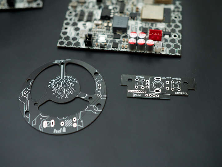
Modern electronics are small and dense, and without skills and special equipment, it is challenging to assemble a circuit that would look great and be reliable. PCB manufacturing and assembly prices are too small to consider doing everything yourself.

Most PCB fab houses are already providing PCB Assembly (PCBA) services. So, if you order a PCB prototype, it is wise to go along with assembly. Let’s look at the JLCPCB manufacturer’s PCB assembly capabilities and pricing options.
PCB assembly capabilities at JLCPCB
Unless you are ordering a particular PCB, it is hardly undoable. The range of possible variations is vast and constantly increasing as the service expands with new technologies and features. JLCBPCB offers packages of PCB assembly. One is called Economic, meaning that this is a super-saving choice where you are limited in choices like PCB color, surface finish, and other parameters. Another option is Standard PCBA, where you get much more flexibility.
Economic PCBA
Economic PCBA package supports only one side component placement 2-, 4- or 6-layer PCBs. PCB thickness ranges from 0.8mm to 1.6mm. The surface finish is limited according to board layers but mainly is lead/lead-free/HASL coating. The PCB color also is limited to green and black. The economic package doesn’t offer Solder Paste Inspection (SPI); however other inspections such as Automatic Optical Inspection (AOI), visual inspection, and X-ray are possible. Also, economic assembly is much faster and can be as fast as 1 to 3 days. Such speed is possible because all parameters are within standard thresholds of mass production.
Standard PCBA
Standard PCBA is more advanced and supports a broader range of features. You are not limited in the choice of PCB layers up to 6. The number of layers is only limited to PCB prototyping capabilities. JLCPCB is not assembling on other manufacturer boards. The assembly will automatically catch up if they upgrade their technology to build more layered PCBs. The board thickness can be as small as 0.4mm up to 2mm. The single PCB can be up to 400x500mm. Also, there is no limit on surface finish and PCB color (green, purple, red, yellow, blue, white, and black). IC spacing can be down to 0.35 and 0.5 for BGA. All possible inspections, including SPI, are present. However, if you choose nonstandard parameters for assembly, it may take more than four days.
PCB assembly pricing at JLCPCB
Turnkey PCB assembly is becoming a cheap option after the PCB prototype. JLCPCB’s current quoted pricing includes:
$8 – setup fee
$1.5 – stencil
$00017 – SMT assembly per joint
$3.5 – hand soldering fee
$0.0173 – Manual assembly per joint
If you are new to JLCPCB, you can register as a new user and get a coupon for your first order. There is a big chance that with discount coupons, your first assembled PCB will be at no cost or a meager fee such as $2.
What to look for when ordering PCBA service at JLCPCB
PCBA service at JLCPCB is relatively new and growing. If you are building a complicated PCB with many different electronics parts, check out their component stock. They have more than 230,000 in stock, ready to be soldered. The library is constantly extending, so there should be no problem with any common component. However, it won’t be soldered if they do not have a particular piece. Currently, they do not accept parts supplied by you.
Another potential issue may be if your part is not in the standard but an extended library. The operator must place the reel manually so that additional charges may apply.
If you use mixed components, manual assembly might be required, leading to additional costs and longer turn-time.
No matter what, all possible issues and concerns can be solved through a support system. They have a dedicated team of over 3000 employees and more than 15 years of expertise in the field.
Take away
PCB assembly is becoming a standard feature after prototyping in the same fab-house. Assembly service frees you from multiple headaches such as where to source components, how to apply the paste, how to place components, how to solder, and how to test if everything is done right. You can focus on other tasks such as designing new electronic devices and getting them ready with a button click.
Read more about JLCPCB services.
