Established in 2006, JLCPCB is the earliest PCB factory focusing prototype and small-batch production in China. More than 350,000+ worldwide customers enjoy the fast and easy PCB fabrication service on JLCPCB. JLCPCB make a video for helping more customers and engineers learn about how to make a 2-layer PCBs in the factory and every step of the process, from Production, Quality Control to Shipping.
Building any sort of electronics project is a multi-step process that involve creating a circuit, testing it, creating PCB, soldering, and checking if everything works as planned. All these steps take significant time, but manufacturing PCB involves some waiting period until board arrives. Of course, you can try to make PCB prototype by yourself, but this process is messy and requires special tools like UV lamps.
Today probably every hobbyist is ordering PCBs online with guarantee of getting professionally looking product. There are many PCB fab houses that offer excellent services. They are wary of offering different pricings, turnaround times, and board varieties. Recently I had a great experience with JLCPCB fabrication house. As a hobbyist, I am looking for a small prices when ordering small batches, short build time, and quality. JLCPCB fab house offer $2 building price for ten boards smaller than 100x100mm and build time of 2 days. Of course, shipping takes the rest, which you cannot control much unless you choose DHL delivery which is costly (~$24). My order came in less than couple weeks from the moment I ordered using regular shipping (~$7).
The ordering process is painless as they have done a great job of building user interface. Practically all you need to do is to upload your zipped Gerber files, and the rest is done automatically.
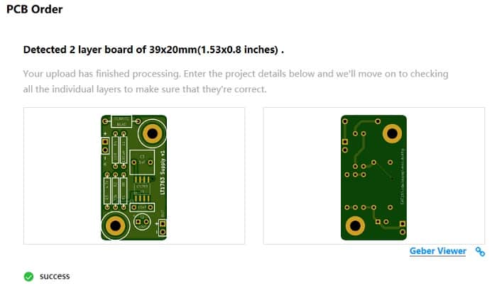
Online Gerber viewer makes it easy to check if everything is done correctly and is safe to order. The system recognizes Gerber files generated by multiple PCB editors such as Altium, Eagle, Kicad, and Diptrace. They even offer online PCB editor and simulator designed by EasyEda, which is suitable for building complex projects.
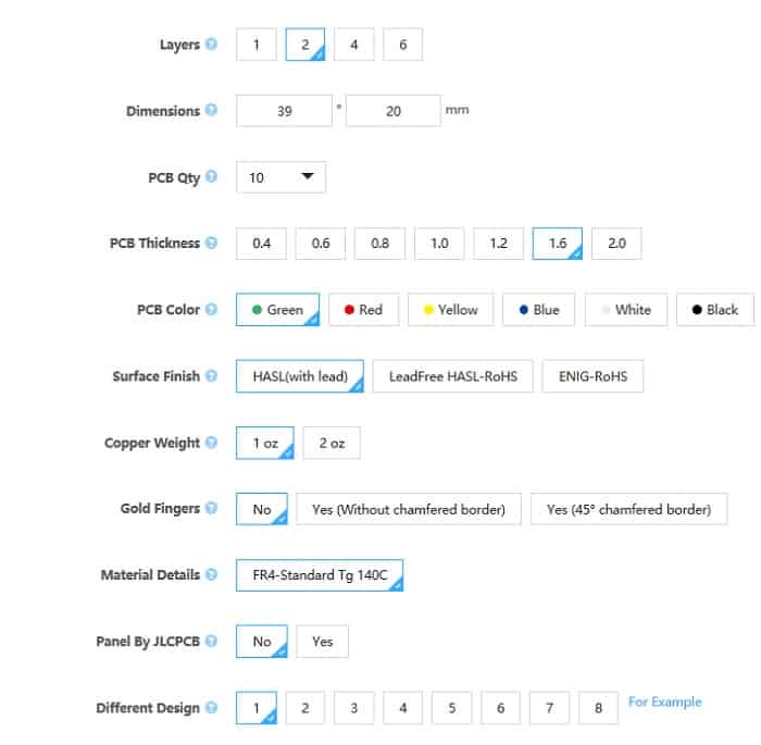
After PCB is imported and detected you are free to select various PCB properties like the color (green, red, yellow, blue, white, and black), different surface finishes, copper weight, material, and so on. Of course, when you drift from default settings the price goes up. In most cases, default selection with lowest price is more than enough unless you want different-looking PCB.
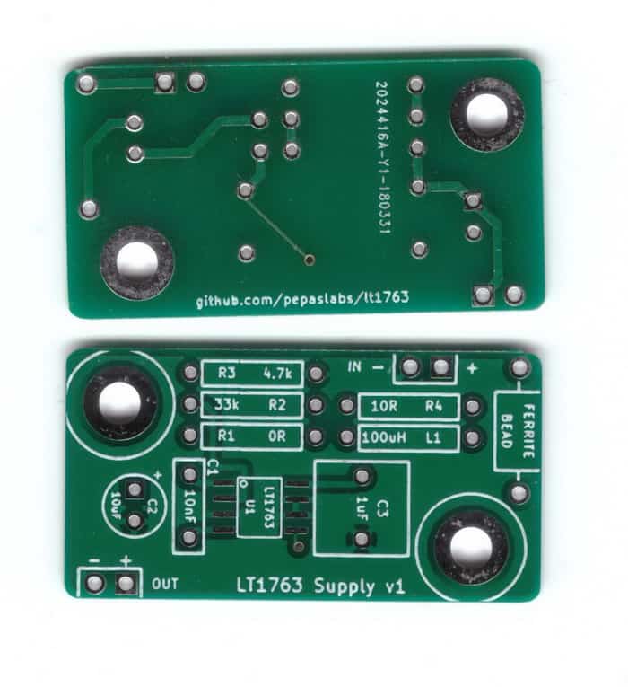
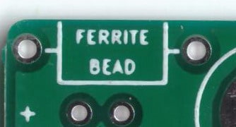
From the first glance, physical PCB boards look quality made. With such slight complexity, it is hard to judge, but it seems that parts placement and silkscreen is well aligned. Soldier resist layer is symmetrical and surrounds pads well.
The text on silk screen is enough to read and understand, but in some places, it could be crisper. This part is not crucial, but I imagine for larger boards with denser component layouts, this might not start to look pretty. But for this price range, this is more than enough, and you can hardly get better results anywhere else.
The routing of boards is excellent – no sharp edges. All batches often PCBs arrive well-made, and I have no problem with ordering again and recommending JLCPCB service to you.
The schematic, PCB, and Gerber files can be found at https://github.com/pepaslabs/lt1763
