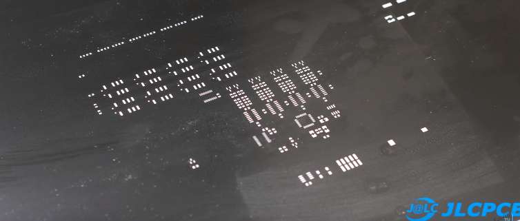
A PCB Stencil is a sheet of stainless steel with laser-cut apertures that we have to use to apply solder paste to a PCB board to insert surface mount components. The PCB stencil has the use to apply solder paste to specific areas on a bare PCB board. So that components can be precisely fitted and aligned.

An SMT stencil’s main purpose is to transfer solder paste to a bare circuit board. Every surface mount device on the board has an aperture created by a laser-cut stainless steel foil.
The ideal size of the stencil aperture is to fit the PCB’s land area. With a standard stencil thickness of 0.125mm, a pad to the aperture aspect ratio of 90 percent to 100 percent is the best one.
PCB stencils are made of metal or polyimide, which is commonly useful for thin sheets. Metal (usually stainless steel) stencils are best for producing a large number of prototypes. Stainless steel stencils enable more precise aperture creation.
A PCB stencil, solder paste stencil, or laser stencil are all terms that have the same meanings to describe a surface mount technology (SMT) stencil. The main purpose of an SMT stencil is to transfer solder paste to a bare circuit board. Each surface mount device on the board has an opening created by a laser-cut stainless steel foil.
What is the PCB stencils manufacturing process?
At the JLCPCB factory the process of stencil manufacturing consists of the following steps.
- PCB Stencils process starts by cutting apertures in a stainless steel foil-base sheet using lasers at the locations where Surface Mount components must insert on the board.
- Then, the stencil is placed on top of the PCB and carefully positioned using fiducial markings.
- After that, a metal squeegee blade is used to apply the solder paste after being aligned.
- As a result, solder paste is applied to the PCB board where surface-mount components have to install.
- Finally, components can be placed on the board once the stencil is removed.
While developing or ordering a PCB stencil, there are some important points to keep in mind. If you are ordering Stencils, you are likely manufacturing a PCB and plan to assemble the board. Why not use a special offer where you can get 1-4 layer PCB manufactured for as low as $2? Additionally, you can get a free coupon for SMT assembly.
1. The thickness of the stainless steel sheet
Stencil sheet’s precise thickness guarantees that the proper amount of solder paste is released. Because excessive solder deposition may create solder bridging. Moreover, the thickness of the sheet and the aperture size are critical criteria that influence the amount of solder paste that has to deposit on the board. On the other hand, insufficient solder deposition can result in weak solder joints, which can compromise the final PCB board’s functionality.
2. The aperture size of the opening created
The stencil aperture is somewhat smaller than the PCB pad size to eliminate solder flaws like bridging and solder beads. Then, there is a chance that the solder paste will migrate to the PCB or stick to the aperture walls of the stencil. To avoid this, the PCB pad should always be larger than two-thirds of the inside aperture wall of the stencil.
3. Stencil Material
The solder paste delivery from the opening/aperture to the PCB pad may also affect the stencil material. Stainless steel is the most used material for stencils.
4. Stencil Alignment

Registration marks are called “fiducial marks.” These fiducial markers ensure that the PCB and stencil have proper alignment. Laser-cut stencils, Chemical-etch stencils, Framed PCB Stencils, Frameless PCB Stencils, and Hybrid PCB Stencils are the different types of PCB stencils on their aperture type and mounting technique.
What are the different types of stencils?
1. Laser-cut Stencils:
A laser beam is useful to cut the openings/apertures in the PCB stencil on a stainless steel sheet. This stencil ensures a high level of accuracy.
2. Chemical-etch stencils:
Acid is useful to etch the openings on the PCB stencil into metal. While such a stencil allows for quick production at a low cost, it does not safeguard the environment from dangerous chemicals.
3. Framed PCB stencils
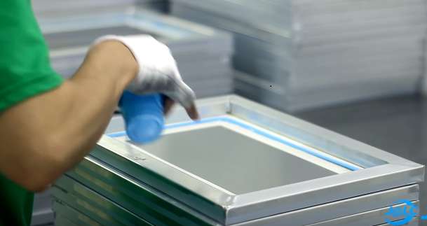
In the case of this type, there is a frame around the stencils. For the frame, a mesh border needs to employ to keep the stencil sheet tight for the desired accuracy. Framed PCB Stencils are useful for high-volume PCB fabrication because they provide constant repeatability and excellent print quality.
4. Reusable PCB Stencils:
There is no fixed frame on such stencils. They have a chance to rearrange into various frames and removed them at any moment. They are less expensive than frameless stencils. These may utilize hand soldering methods and take up less storage space.
5. Prototype or Photo Stencils:
These stencils are based on a custom-made design created with a CAD or Gerber file. These are useful to practice manual printing and ideas.
6. PCB Hybrid Stencils:
A hybrid stencil combines chemically etched and laser-cut stencils.
What do you know about the purposes of PCB stencils?
There are many purposes of PCB stencils. All the purposes are not possible to write here that’s why some of them are here.
- Firstly, the primary goal of utilizing SMT stencils is to make it easier to place a component onto a board once it has been coated with solder paste.
- Secondly, by minimizing the manual positioning of components, power stencils help to reduce labor costs and lead time.
- Then these are thus regarded as a godsend for mass production of the same PCB.
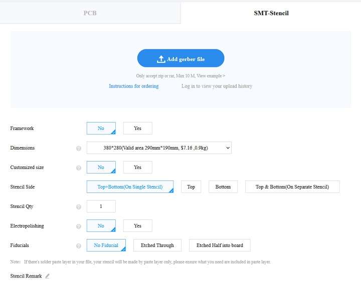
- Furthermore, at JLCPCB, SMT stencils are available in two styles: having frame and frameless.
- Although framed stencils have better suited for high volume print circuit boards.
- While frameless stencils are preferable in a high-mix scenario due to their ease of replacement.
What is electropolishing?
Electropolishing removes small burrs, improves surface quality, and smooth the interior walls for improved paste release. This technique is mostly fruitful on ICs with less than 0.5mm lead width and BGA chips.


