Imagine the vast amount of electronics that have been built over the years. There is always a human behind each design and product. Modern technologies allow to automate designing, building, and fabrication processes at some degree, but everything has to orchestrate by a knowledgeable person who knows how to set things up and ensure a smooth transition from idea to a working model.
Manufacturing any functionality and shape is not a problem anymore, because many sophisticated technologies do wonders in the right hands. The only thing that is needed is the idea. If you are good at generating amazing ideas, the rest can be done without your intervention. The PCBWay is capable of taking the rest from your idea.
Many exciting concepts would be exciting or valuable to fulfill but sometimes lack effort or time they never reach daylight. It takes time and significant effort to design new devices from start to finish. Why not leave labor-intensive tasks to people who are good at what they do and let your imagination take over.
PCBWay is taking a step further and offering PCB Layout service, where a team of skilled engineers can lay out your design according to modern technology standards. Depending on design complexity, you may need to provide a schematic or design logic using one of the popular EAD software formats, such as Power PCB, ORCAD, AutoCAD, and CAM350. I am sure that with open for communication, there is no limitation on what tool to use. There is a good chance that they will draw schematic, lay out a PCB, fabricate it, and assemble in one go. The team of engineers is working day to day with schematics and PCBs, and their experience far better than yours.

The PCBWay offer incredibly diverse services:
- Electronic design, including technical management of the whole project. They use popular EAD software for building, managing, and documenting projects. A partnership with product design companies offers a wide range of high-quality services from start to finish.
- Financial management of the project. Keeping track of budgets and costs remotely may not be convenient. All the ongoing cash flow is managed effectively on-site.
- Firmware programming, implementation, and IT management. They are capable of offering a wide range of software and firmware development. Experienced teams can program embedded devices according to your specs or general concepts. There is no limit on platforms, whether it is a Windows, Linux, Mac OS, or Android application.
- Mechanical design of the project, including 3D modeling and realization. The design should not be left without an enclosure. It may fit into any shape and form that can be produced by mold injection or even 3D milled or printed.
- Documentation from start to finish. The documentation of the project and the final device is as necessary as the prototype itself. This part is taken care of with professional attitude and requirements.
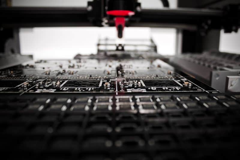
The PCB layout can be done according to PCB fabrication capabilities. The maximum number of layers can be up to 40; max pins 6000, min spacing 0.2mm. The highest signal speeds up to 12GHz, EMI protection, BGA, high currents, and power supplies.
The layout process time depends on complexity. It may start from 3-5 days for simple designs and take up to a month for complex projects. You can always do more work before applying to speed up the processes.
The electronic design takes valuable human time and professionalism. Usually, the whole process involves multiple teams that may involve third-party professionals. It may take a significant initial investment, but in the long run, design and layout services may save tons of time and money. For more information, please visit PCBWay webpage.